AsiaTechDaily – Asia's Leading Tech and Startup Media Platform

Why Deep-Tech Startups Are Targeting the “Small” Bottlenecks Behind AI’s Biggest Costs
 by
by

As AI infrastructure becomes constrained by power, heat and packaging, a new generation of deep-tech startups is targeting efficiency gains at the material and component level, where seemingly small improvements can affect the economics of entire computing systems.
The next constraint on AI infrastructure may not be another AI model or accelerator. It may be the physical layers that allow increasingly powerful chips to operate. Global data center electricity consumption increased 17% in 2025, while electricity use by AI-focused data centers rose by 50%, according to the International Energy Agency. The IEA also estimates that the power density of AI servers increased 11-fold between 2020 and 2025 and could rise another fourfold by 2027. An individual advanced server rack could then have peak power demand equivalent to roughly 65 households.
Those numbers are changing what efficiency means in AI. Improving model performance is only part of the equation. More compute requires more electricity, while higher power density creates more heat that has to be removed. At the chip level, advanced packaging is becoming increasingly important because processors, memory and chiplets are being packed closer together to move data faster and more efficiently.
This is creating an opportunity for deep-tech companies that are not trying to replace the AI infrastructure stack, but improve the small interfaces and components within it.
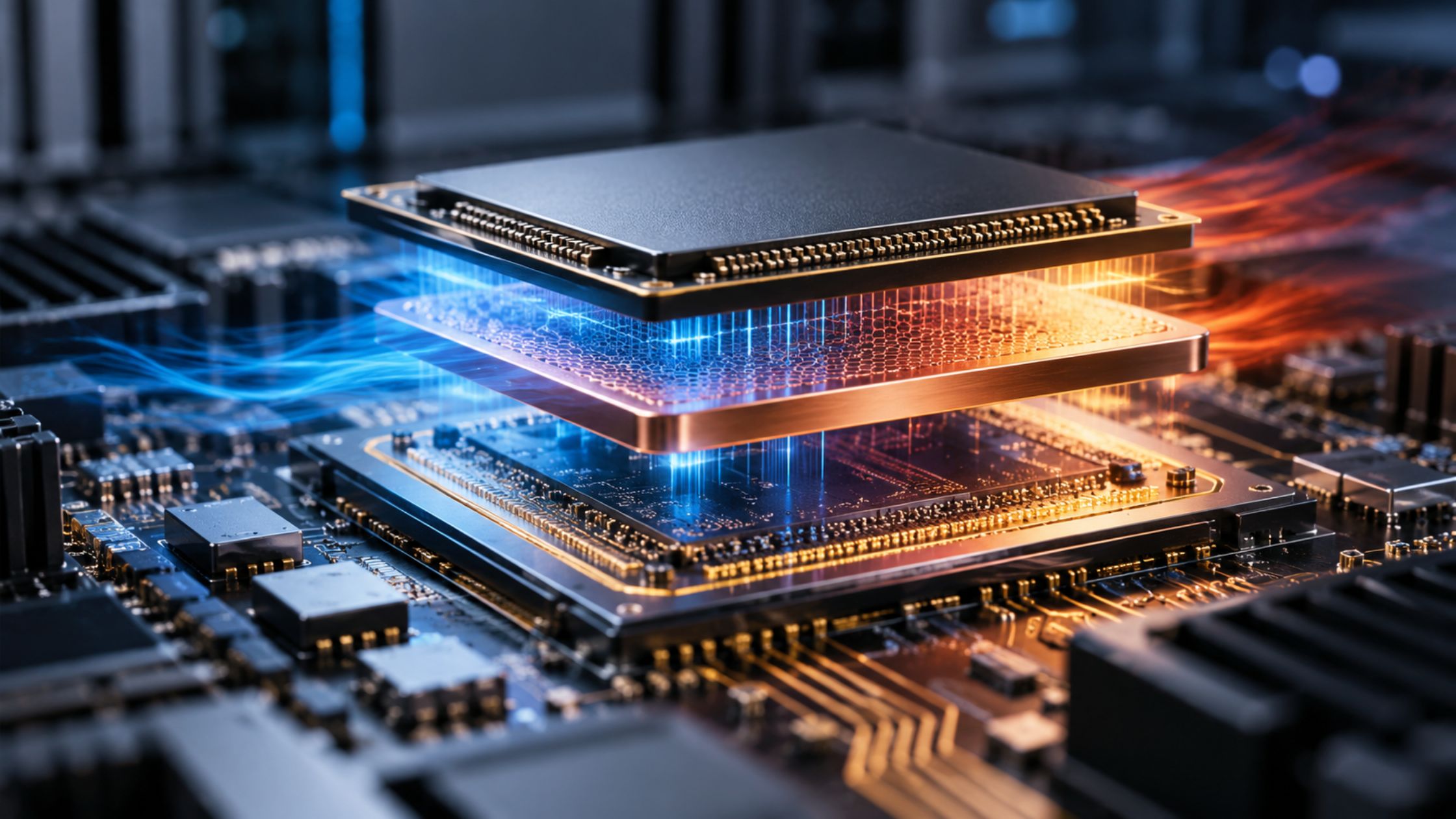
As AI accelerators become more powerful, the semiconductor package is increasingly becoming a performance constraint. Modern AI packages combine compute, high-bandwidth memory and dense interconnects within increasingly small physical spaces. That concentration increases electrical and thermal loads, making power delivery and heat dissipation harder to manage. Industry analysis now points to advanced packaging, thermal interfaces, power delivery and cooling as interconnected constraints on AI scaling.
This matters because inefficiency at the component level does not stay at the component level. An electrical loss becomes heat. Heat requires cooling. Cooling consumes additional energy and infrastructure. Thermal constraints can also limit how aggressively a system can operate. That creates a multiplier effect around what might initially look like a small materials problem.
Why Improving the Interface Can Matter
Malaysian deep-tech startup nanoSkunkWorkX, or nSWX, is approaching this problem through the interface between materials. Its lead product, nSD-I, uses a graphene-copper thin-film interface designed to improve how current and heat move through copper structures inside advanced AI chip packages. The company says its peer-reviewed work found that its graphene-copper films can move heat across their surface at more than twice the rate of a copper baseline, with follow-up testing showing the performance advantage remained after use in pre-qualification components.
The important proposition is not replacing copper or forcing semiconductor manufacturers to rebuild their production infrastructure. nSWX is attempting to improve the performance of an existing material and manufacturing ecosystem. That approach reflects a broader direction in semiconductor engineering. Advanced packaging is already becoming a critical enabler of AI scaling, but increasing density introduces manufacturing and thermal-management challenges that require improvements across multiple layers of the package.
Iqbal Shamsul, Co-Founder and CEO of nanoSkunkWorkX, explained the commercial opportunity while conversing with AsiaTechDaily:
“Every watt of electrical loss inside the package becomes heat the rest of the AI system has to pay to manage. The immediate opportunity is inside the chip package. Copper there has to carry more power, move more signals, and handle more heat through tighter spaces. If the gains we have already measured survive package qualification, customers get something valuable: margin. They can spend that margin on more current, denser designs, lower heat, greater reliability, or less cooling and infrastructure overhead. At AI-infrastructure scale, that is the opportunity we see: more useful compute from the same power and infrastructure, and ultimately a lower cost per useful AI workload. Current nSWX materials frame that as the economic target, while keeping package conversion and qualification as the next proof gate.”
The word “margin” is important. For an AI infrastructure operator, an efficiency improvement does not necessarily have to translate into a single headline performance metric. It can create flexibility across the system, allowing operators to increase compute density, reduce cooling requirements, improve reliability or lower the cost of running workloads.
The Economics of Small Efficiency Gains
The growing attention to component-level efficiency is partly a response to the scale of AI infrastructure spending. The IEA reported that capital expenditure by five major technology companies exceeded $400 billion in 2025 and is expected to increase by another 75% in 2026. At the same time, AI-focused data center electricity consumption grew much faster than overall global electricity demand. When infrastructure operates at this scale, a small efficiency improvement can have a much larger economic consequence if it is applied across enough systems.
This is also why companies are attacking the problem from multiple directions. Research published in 2026, for example, found that optimized liquid-to-chip cooling could potentially reduce peak energy demand by 6% to 14% and annual energy consumption by 4% to 13% under the study’s modeled conditions. The emerging market is therefore not simply about building more powerful chips. It is about improving everything that allows those chips to deliver useful compute efficiently.
The Hard Part Is Proving It Inside the Industry
For deep-tech startups, however, identifying a bottleneck is only the beginning. nSWX has developed its core platform, three product lines and initial revenue with less than $1.5 million in external pre-seed capital. Its latest $2 million seed round, led by Singapore-based Tin Men Capital, is intended to move nSD-I toward semiconductor partner qualification and scale its interface-engineering platform.
That qualification stage is critical. A materials technology can demonstrate strong laboratory performance and still face questions around manufacturing compatibility, reliability, process integration, consistency and economics. nSWX’s strategy is therefore to develop a technology that can work within the manufacturing infrastructure already used by the semiconductor industry. The company’s broader SUSANNE platform is designed to create controlled interfaces within existing manufacturing and device flows, while its semiconductor product represents the first commercial application of that capability.
Its presentation of graphene-copper work at IEEE EPEPS 2025 also reflects the importance of peer-reviewed validation as the company moves toward industrial qualification.
The AI infrastructure race has largely been described through GPUs, data centers and power generation. Increasingly, however, the constraints are becoming more granular. Power delivery, thermal interfaces, advanced packaging, cooling and materials all determine how much of the theoretical capability of an AI accelerator can actually become useful compute. That changes the opportunity for deep-tech startups. They do not necessarily need to build the next processor to participate in AI’s growth. They can target the physical bottlenecks that limit what existing processors can deliver.
For nSWX, the immediate test is whether its interface technology can move from promising material-level results through semiconductor qualification and into commercial packages. If it can, the value proposition extends beyond a better material: it becomes a way of extracting more useful compute from infrastructure that the industry is already spending billions to build.
As AI systems become larger and more power-intensive, the next generation of efficiency gains may increasingly come from small engineering improvements at the boundaries between components. The challenge for deep-tech startups will be proving that those small gains can survive the transition from laboratory performance to industrial-scale economics.
Quick Takeaways
- AI’s next bottleneck is increasingly physical: Power, heat, cooling, packaging, and power delivery are becoming constraints as AI infrastructure scales.
- Small component-level gains can have system-wide effects: Reducing electrical losses can lower heat generation, cooling requirements, and infrastructure costs.
- Advanced packaging is becoming critical: As compute, memory, and interconnects are packed closer together, material interfaces can directly influence performance and reliability.
- Deep-tech startups are targeting the “in-between” layers: Instead of competing with chipmakers, companies such as nanoSkunkWorkX (nSWX) are improving existing materials and manufacturing processes.
- The economic value is flexibility, not just efficiency: A component-level improvement can give operators more room for higher compute density, lower temperatures, improved reliability, or reduced cooling overhead.
- Scale makes small gains meaningful: With AI infrastructure requiring hundreds of billions of dollars in annual capital investment and rapidly increasing electricity demand, even modest efficiency improvements can have significant cumulative effects.
- Qualification is the key commercial hurdle: Laboratory and peer-reviewed results are only the starting point. Deep-tech companies must prove reliability, manufacturing compatibility, consistency, and economics inside real semiconductor production environments.
- nSWX is moving toward that next stage: Its $2 million seed round is aimed at advancing its nSD-I interface technology toward semiconductor partner qualification and scaling its broader interface-engineering platform.
- The broader trend: AI infrastructure innovation is expanding beyond GPUs and data centers into materials, packaging, cooling, power delivery, and thermal management.
- Core takeaway: The next meaningful AI efficiency gains may come not from making the biggest component better, but from removing the small physical inefficiencies that limit the entire system.