AsiaTechDaily – Asia's Leading Tech and Startup Media Platform

Malaysian Deep-Tech Startup nanoSkunkWorkX Raises US$2M to Qualify AI Chip Packaging Interface
 by
by

The Tin Men Capital-led round will move nSWX’s graphene-copper interface toward semiconductor partner qualification as Malaysia pushes deeper into advanced packaging.
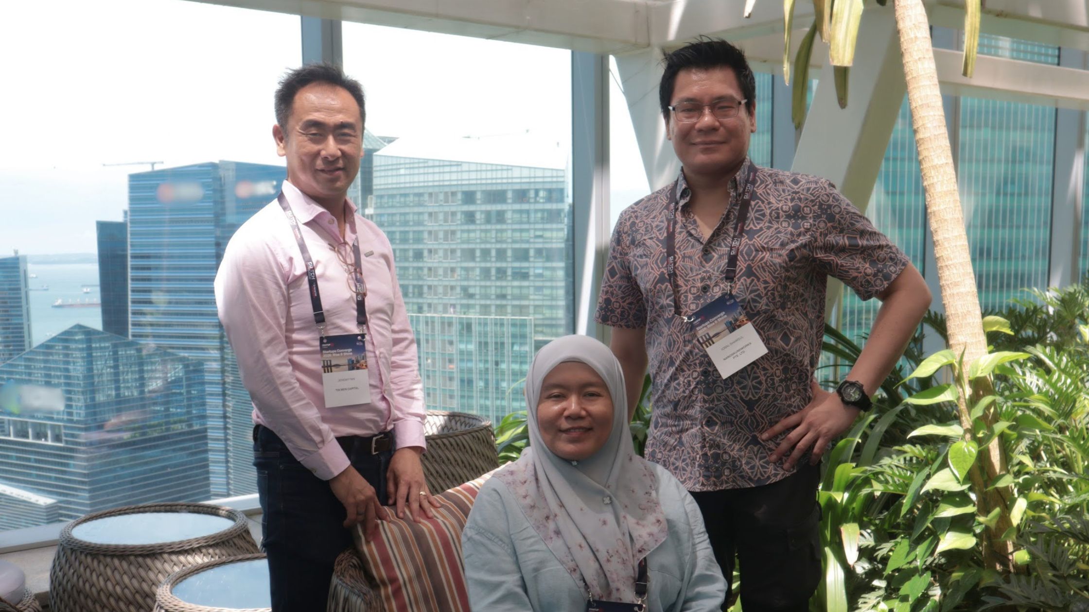
Malaysian deep-tech startup nanoSkunkWorkX (nSWX) has raised US$2 million in a seed round led by Singapore-based frontier technology venture capital firm Tin Men Capital, as the company moves its materials technology toward qualification for advanced semiconductor packaging. The funding comes as thermal management and power efficiency become increasingly important constraints in AI hardware. Advanced packaging is playing a larger role in AI and high-performance computing as chiplets, high-bandwidth memory and increasingly dense package architectures place greater demands on electrical, thermal and mechanical performance. Industry research now treats thermal integrity, power integrity and reliability as interconnected packaging challenges rather than isolated engineering problems.
nSWX’s immediate focus is its nSD-I interface, a thin-film technology designed to help copper interconnects in AI chip packages carry more current while improving heat dissipation. The company says its approach is intended to work without replacing copper or requiring changes to the surrounding manufacturing process.
The round is Tin Men Capital’s first investment in a Malaysian startup and builds on previous backing from Gobi Dana Impak and Malaysia’s Kumpulan Modal Perdana. nSWX said it has developed its core platform, three product lines, peer-reviewed semiconductor data and generated its first revenue with less than US$1.5 million in cumulative external pre-seed capital.
From demonstrating an effect to qualifying a process
For nSWX, the more consequential milestone is not demonstrating that its material can improve thermal performance. It is determining whether that improvement can be reproduced within the tightly controlled processes used to manufacture advanced semiconductor packages. While conversing with AsiaTechDaily, Iqbal Shamsul, Co-Founder and CEO of nanoSkunkWorkX, said the company has moved beyond the initial proof-of-effect stage.
“We are past proving the effect exists. The next job is proving that the process works reliably inside the customer’s manufacturing flow. We have shown the gains at lab and development scale, including in microelectronics test structures that begin to resemble the circuits used in advanced packaging. Now we scale that interface-engineering process to deployment-relevant wafers and partner manufacturing flows. We are already scoping evaluations with players across the advanced-packaging ecosystem.
The remaining gates are clear: representative package test vehicles, process integration, reliability, repeatability, larger-wafer scale, and a qualified process window with an industry partner. In semiconductors, commercialisation is not just a better material. The material architecture and the process that forms it have to work, repeatedly, inside an existing production flow. That qualification boundary is consistent with the current nSWX commercial path.”
That qualification challenge is significant because semiconductor manufacturers cannot adopt materials solely on the basis of laboratory performance. Reliability, repeatability, process compatibility, wafer-scale production and yield all determine whether a materials innovation can move into commercial manufacturing.
nSWX’s nSD-I uses a graphene-copper film architecture. According to the company, peer-reviewed work found that its films could move heat across their surface more than twice as effectively as a copper baseline. Follow-up testing reportedly showed that the performance advantage remained after use in pre-qualification test components. The company argues that improvements at this interface could potentially reduce thermal throttling and cooling requirements while improving compute efficiency. Those downstream benefits, however, will depend on whether the technology can meet the qualification and manufacturing requirements outlined by Shamsul.
Malaysia’s semiconductor position is shifting
The development also comes as Malaysia attempts to move beyond its established role in semiconductor assembly, testing and packaging toward higher-value activities. The Malaysian Investment Development Authority estimates that the country accounts for about 13% of global assembly, testing and packaging volume and ranks as the world’s sixth-largest semiconductor exporter. Malaysia is now targeting areas including IC design, advanced packaging and digitally enabled manufacturing as part of its broader semiconductor strategy.
The shift is already attracting investment in advanced packaging infrastructure. Malaysia’s electrical and electronics sector secured RM28.5 billion in approved investments in 2025, while government and industry initiatives are increasingly focused on moving local capabilities further up the semiconductor value chain. For nSWX, that ecosystem provides a potential route for a Malaysian materials company to participate in a part of the semiconductor value chain where performance improvements can have system-level consequences.
“At scale, performance breaks at the boundaries between materials. Heat, charge, and signals concentrate where one material meets another, and that is where many critical losses in modern systems occur. Our thesis is that improving a small, critical interface can unlock much larger system gains while preserving the materials, equipment and manufacturing base already around it,” said Dr Amani Salim, Co-Founder and CTO of nanoSkunkWorkX, in the company’s announcement.
nSWX was also selected for the inaugural SemiconStart Malaysia cohort, led by MTDC with Silicon Catalyst UK, to advance package qualification and access to the global semiconductor industry. The company was a finalist in the Baker Hughes Energy Ideas Generation Program APAC in 2025.
Beyond AI chips
Although semiconductor packaging is now the lead commercial focus, nSWX is applying the same interface-engineering approach to other areas. In green hydrogen, the company is working to improve charge transfer while reducing reliance on platinum-group metals. Its diagnostics programme is being developed through a paid joint R&D agreement with the US Navy’s Naval Medical Research Unit INDO PACIFIC for biosensors. The funding will support these validation programmes alongside semiconductor qualification, process-platform scale-up, strategic hiring and intellectual property development.
While conversing with AsiaTechDaily, Dr Salim said the next phase will focus on turning the technology into something industry partners can evaluate and eventually adopt.
“The US$2 million seed round will help nSWX move into its next phase of growth, with a focus on industry validation, scale-up, strategic hires and strengthening our IP portfolio. Our key milestones are to validate the technology with industry partners, build the capabilities needed for broader commercial adoption, bring in critical talent to support execution, and continue expanding the intellectual property that underpins our competitive advantage. Ultimately, this round is about positioning nSWX for the next stage of commercialisation and growth.”
The investment therefore marks a transition point for nSWX rather than the end of its technology-development journey. The company’s next test is whether a materials innovation demonstrated at development scale can satisfy the reliability, integration and repeatability requirements of semiconductor manufacturing.
That distinction will determine whether a relatively small improvement at a copper interface can translate into a meaningful role in the rapidly expanding AI hardware stack.
Quick Takeaways
- nanoSkunkWorkX raised US$2 million in seed funding led by Singapore-based Tin Men Capital, with earlier backing from Gobi Dana Impak and Kumpulan Modal Perdana.
- The Malaysian startup is targeting a key AI chip packaging challenge: managing heat and current as semiconductor packages become increasingly dense.
- Its nSD-I graphene-copper interface is designed to improve thermal and electrical performance without replacing existing copper infrastructure.
- The company has moved beyond laboratory proof and is now working toward semiconductor partner qualification, including wafer-scale testing, process integration, reliability and repeatability.
- The funding will support industry validation, process scale-up, strategic hiring, IP development, and hydrogen and diagnostics programs across Asia.
- The development comes as Malaysia seeks to move higher up the semiconductor value chain, expanding beyond its established assembly, testing and packaging base.
- nSWX is also developing applications for green hydrogen and rapid diagnostics, including a paid R&D program with the US Navy’s NAMRU INDO PACIFIC.
- The next major test for the company will be whether its materials technology can transition from development-stage performance to repeatable, manufacturable semiconductor technology.
Similar Articles